Loading page, please wait…
India Plans USD 15 Billion for Chipmaking - UPSC Economy
What is India Plans USD 15 Billion for Chipmaking in UPSC Economy?
India Plans USD 15 Billion for Chipmaking is a key topic under Economy for UPSC Civil Services Examination. Key points include: India commits USD 15 billion for Phase II of chip manufacturing incentives.. Total commitment for chipmaking incentives now stands at USD 25 billion (USD 10B Phase I + USD 15B Phase II).. Three ATMP/OSAT plants approved, less complex than fabrication units.. Understanding this topic is essential for both UPSC Prelims and Mains preparation.
Why is India Plans USD 15 Billion for Chipmaking important for UPSC exam?
India Plans USD 15 Billion for Chipmaking is a Medium-level topic in UPSC Economy. It is tested in both Prelims (factual MCQs) and Mains (analytical answer writing). Previous year UPSC questions have frequently covered aspects of India Plans USD 15 Billion for Chipmaking, making it essential for comprehensive IAS preparation.
How to prepare India Plans USD 15 Billion for Chipmaking for UPSC?
To prepare India Plans USD 15 Billion for Chipmaking for UPSC: (1) Study the comprehensive notes covering all key concepts on Vaidra. (2) Practice previous year questions on this topic. (3) Connect it with current affairs using daily updates. (4) Revise using key takeaways and mind maps available for Economy. (5) Write practice answers linking India Plans USD 15 Billion for Chipmaking to related GS Paper topics.
Key takeaways of India Plans USD 15 Billion for Chipmaking for UPSC
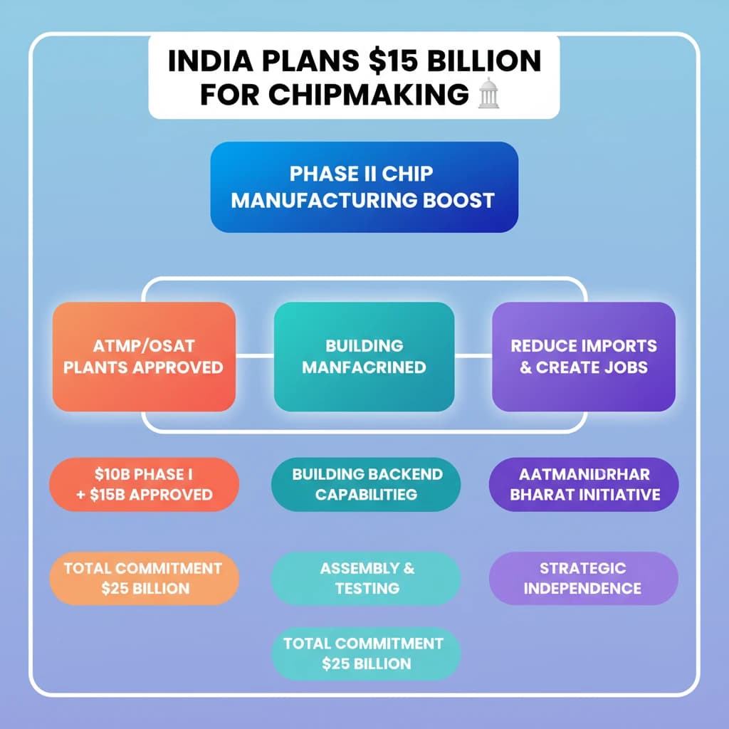
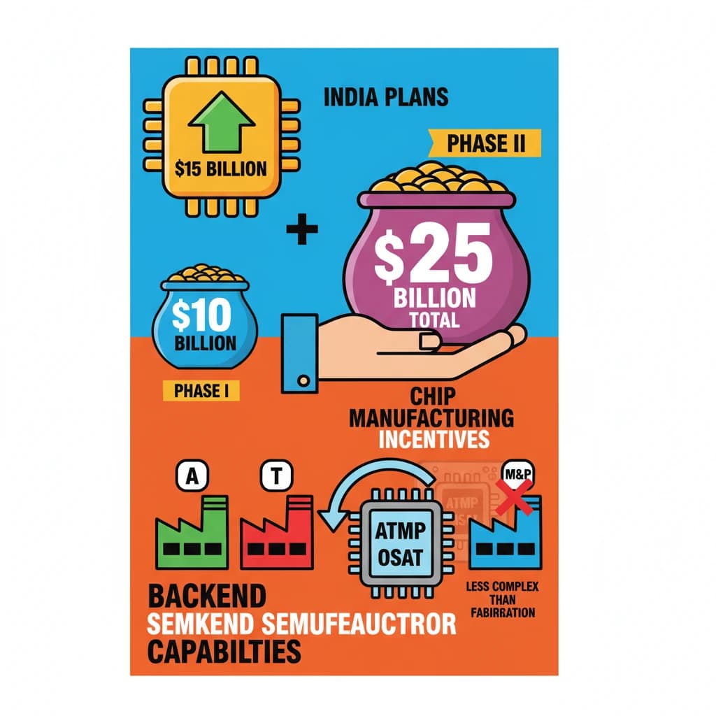
- India commits USD 15 billion for Phase II of chip manufacturing incentives.
- Total commitment for chipmaking incentives now stands at USD 25 billion (USD 10B Phase I + USD 15B Phase II).
- Three ATMP/OSAT plants approved, less complex than fabrication units.
- Focus on building backend semiconductor capabilities (Assembly, Testing, Marking, Packaging).
- Aims to boost Aatmanirbhar Bharat, reduce import dependence, and create jobs.
- Strategic move for India's digital economy and national security.
India Plans USD 15 Billion for Chipmaking
Medium⏱️ 7 min read
economy
📖 Introduction
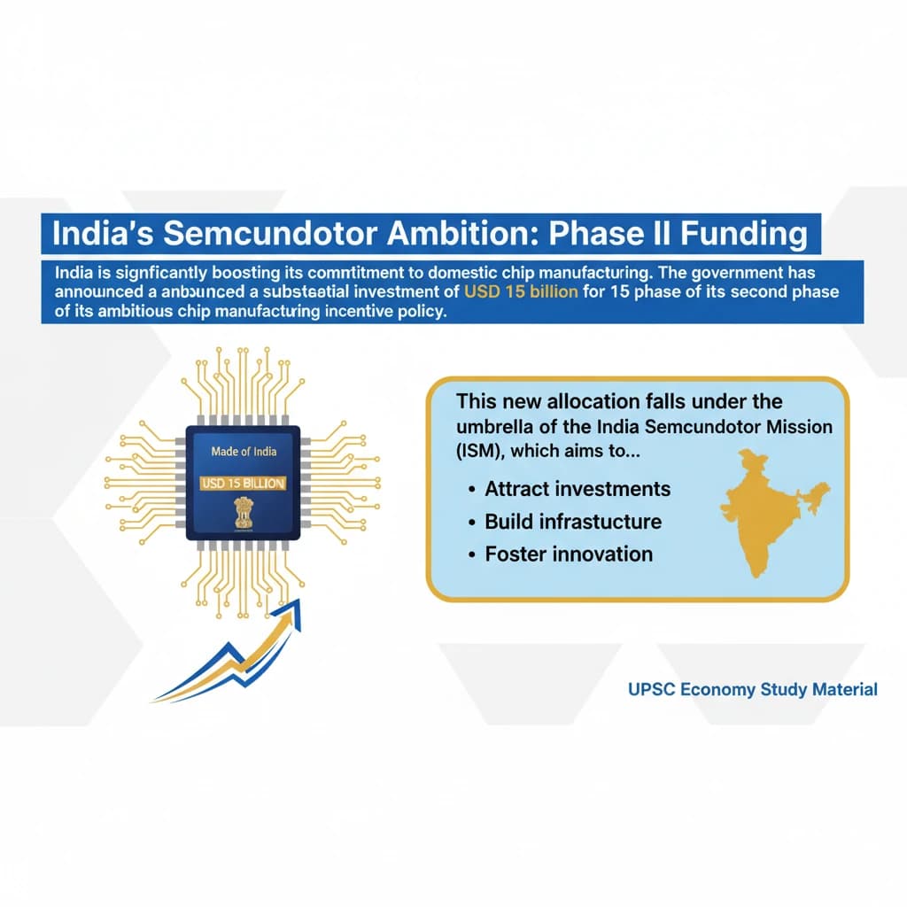
India's Semiconductor Ambition: Phase II Funding
India is significantly boosting its commitment to domestic chip manufacturing. The government has announced a substantial investment of USD 15 billion for the second phase of its ambitious chip manufacturing incentive policy.
This new allocation falls under the umbrella of the India Semiconductor Mission (ISM), which aims to establish India as a global hub for semiconductor design and manufacturing.
This commitment follows an initial pledge of USD 10 billion that was allocated for the first phase of the scheme. The continuous investment underscores the nation's strategic focus on achieving self-reliance in this critical sector.
Approval of ATMP and OSAT Plants
In a related development, the government has also given its approval for the establishment of three assembly and testing plants. These facilities are crucial for the downstream processes of chip production.
These plants are technically referred to as Assembly, Testing, Marking, and Packaging (ATMP) and Outsourced Semiconductor Assembly and Test (OSAT) units. They represent a vital step in building a comprehensive semiconductor ecosystem.
It is important to note that ATMP/OSAT plants are generally less complex to set up and operate compared to full-fledged fabrication plants (fabs). Fabs are responsible for the intricate process of manufacturing the semiconductor wafers themselves.
UPSC Insight: Understanding the distinction between fabrication plants and ATMP/OSAT units is crucial for Mains answers (GS-III Economy). The government's strategy often involves building capabilities in less complex areas first to attract further investment in advanced manufacturing.
💡 Key Takeaways
- •India commits USD 15 billion for Phase II of chip manufacturing incentives.
- •Total commitment for chipmaking incentives now stands at USD 25 billion (USD 10B Phase I + USD 15B Phase II).
- •Three ATMP/OSAT plants approved, less complex than fabrication units.
- •Focus on building backend semiconductor capabilities (Assembly, Testing, Marking, Packaging).
- •Aims to boost Aatmanirbhar Bharat, reduce import dependence, and create jobs.
- •Strategic move for India's digital economy and national security.
🧠 Memory Techniques
95% Verified Content
📚 Reference Sources
•Ministry of Electronics and Information Technology (MeitY) official press releases on India Semiconductor Mission (ISM)
•Press Information Bureau (PIB) releases regarding semiconductor policy and approvals